In the era of electronic miniaturization, Chip-on-Board (COB) technology has become a critical foundation for devices ranging from smartphones and wearables to automotive and industrial control systems. However, directly mounting bare semiconductor dies onto printed circuit boards (PCBs) without traditional plastic packaging makes them highly vulnerable to environmental stress and mechanical damage. This article provides an in-depth analysis of COB chip protection solutions using encapsulation adhesives, highlighting how advanced encapsulant materials help ensure long-term device reliability, stability, and performance.
Solution Summary
Protecting COB chips is far more than simply applying a layer of adhesive over electronic components. It is a sophisticated integration of material science, process engineering, and deep understanding of the operating environment. An optimal protection solution must achieve the right balance between environmental resistance, thermal stability, and manufacturing cost efficiency.
By selecting the appropriate encapsulation method — such as Glob Top or Dam & Fill — together with suitable material chemistries including Epoxy, Silicone, or UV-curable systems, manufacturers can ensure their electronic devices deliver not only excellent laboratory performance, but also long-term durability throughout the product lifecycle.
HITTA proudly introduces advanced solutions from EVERWIDE.
COB chip protection applications have become well established across the electronics industry, and EVERWIDE has successfully implemented COB protection solutions in control boards for one of the market’s leading printer brands, with proven stable operation for more than ten years.
In Dam & Fill applications, EVERWIDE has also overcome the common issue of adhesive warpage. Even after full coating and curing on PCB substrates measuring 60 mm × 60 mm × 0.3 mm, the diagonal warpage remains below 0.1 mm, demonstrating outstanding dimensional stability and process reliability.
Contact Information
HITTA is currently a trusted provider of advanced adhesive and assembly tape solutions from leading global brands. Backed by a highly experienced technical team with hands-on expertise across multiple industries, we deliver not only products, but also optimized bonding solutions tailored to specific application requirements and manufacturing challenges.
If you are seeking an efficient, durable, and reliable bonding solution, HITTA is ready to support you from consultation to implementation.
Contact HITTA today for the most suitable solution.
☎️ Hotline: 0565.336.879
✉️ Email: hittajsc@hitta.vn
Why Do COB Chips Require Specialized Protection Solutions?
COB (Chip-on-Board) technology enables more compact electronic designs by reducing both the footprint and profile of component assemblies through the elimination of traditional chip packaging. Instead, bare silicon dies are mounted directly onto printed circuit boards (PCBs) and electrically connected using ultra-fine gold or aluminum wire bonds.
However, without a conventional protective package, the bare chip and bonding wires become highly vulnerable to environmental and mechanical damage.
Potential Risks to Bare COB Chips
- Chemical Corrosion: Moisture and airborne chemicals can react with chip surfaces and bonding wires, potentially causing short circuits or open circuits.
- Mechanical Stress: Handling during manufacturing or vibration during operation may crack the silicon die or damage delicate wire bonds.
- Thermal Shock: Rapid temperature fluctuations can create uneven expansion and contraction between materials, resulting in structural failure over time.
For this reason, the use of COB protective encapsulation adhesives is not merely optional — it is an essential requirement to create an in-place “protective package” for the electronic assembly.
COB Chip Protection Solutions
Depending on size requirements, dispensing precision, and operating environment, two primary liquid encapsulation methods are commonly used.
Glob Top Solution (Drop-Type Encapsulation Adhesive)
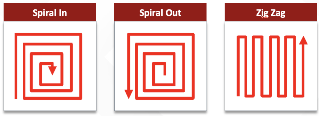
The Glob Top process is one of the two primary methods — alongside Dam & Fill — used to encapsulate and protect bare dies mounted directly onto printed circuit boards in COB applications. Below is a detailed overview of its material characteristics, dispensing process, and application advantages.
Principle and Material Characteristics
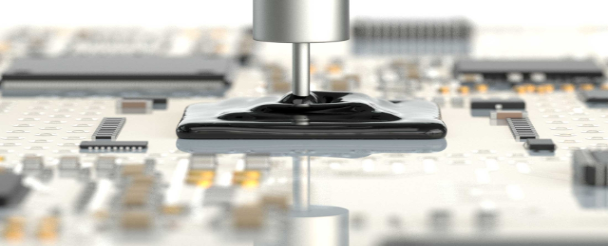
Glob Top is a process in which a liquid encapsulation material is dispensed directly over the silicon die and delicate wire bonds.
- Thixotropic Behavior: This is one of the most critical material properties. The adhesive is engineered to flow easily under dispensing pressure, then rapidly increase in viscosity once deposited on the substrate. This allows the material to penetrate narrow gaps while preventing overflow beyond the target area.
- Fillers: Glob Top materials are commonly formulated with silica or alumina fillers to optimize the Coefficient of Thermal Expansion (CTE). Lowering the CTE helps the encapsulant expand and contract more consistently with the silicon die and PCB, thereby reducing thermal stress that could lead to cracking or wire bond failure.
- Ionic Purity: High-quality Glob Top materials must contain extremely low ionic contamination to minimize the risk of electrochemical corrosion under humid operating conditions.
Adhesive Dispensing Process
The reliability of the Glob Top process depends heavily on dispensing precision and process control.
- Syringe Valve Systems: The simplest dispensing method, using pneumatic pressure to push material through a needle.
- Auger Pump Systems: Utilize shear force to temporarily reduce viscosity during dispensing, enabling more stable flow control for high-viscosity materials.
- True Positive Displacement Pumps: The most precise dispensing technology, delivering a fixed adhesive volume independent of viscosity or temperature variation.
- Preheating: PCBs are commonly heated to approximately 60–110°C before dispensing. This improves material flow around wire bonds, helps eliminate trapped air pockets, and reduces the formation of voids.
Advantages and Limitations
Advantages
- Comprehensive Protection: Forms a durable protective barrier against impact, vibration, moisture, and chemical exposure.
- Wire Bond Protection: Unlike transfer molding, Glob Top minimizes the risk of wire sweep, where ultra-fine bonding wires shift and create electrical shorts.
- Space Saving: Enables maximum miniaturization compared to conventional plastic packaging methods.
Limitations
- Shape Control: Glob Top materials naturally form a dome-shaped profile, making height and surface flatness more difficult to control precisely.
- Void Formation Risk: Without strict process control, trapped air bubbles may remain inside the encapsulant and cause reliability failures under thermal stress.
Comparison with Dam & Fill Technology
Although both methods serve the same purpose of protecting COB assemblies, Glob Top differs from Dam & Fill in several important aspects:
- Process Structure: Glob Top is a simpler one-step encapsulation process, while Dam & Fill is a two-step method involving dam formation followed by cavity filling.
- Surface Flatness: Dam & Fill provides a flatter and more uniform surface profile, making it suitable for ultra-thin electronic devices such as smart cards.
- Penetration Capability: Fill materials used in Dam & Fill systems generally have lower viscosity than Glob Top compounds, allowing better penetration beneath chips and wire bonds.
Dam & Fill Solution (Dam-and-Fill Encapsulation Technology)
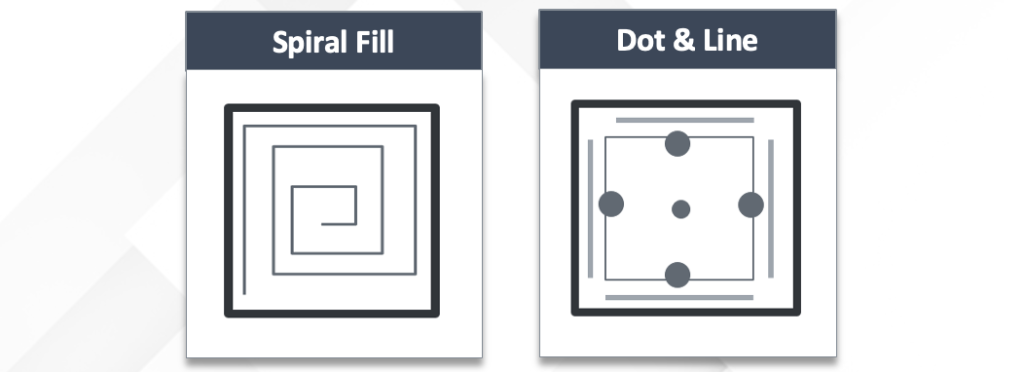
Unlike the Glob Top process, which typically forms a dome-shaped encapsulation with limited height control, Dam & Fill technology provides superior control over package geometry and surface flatness.
Two-Step Process Principle
This method utilizes two encapsulation materials with different flow characteristics to create a highly controlled protective structure. The process is typically performed using automated dispensing systems to ensure maximum precision.
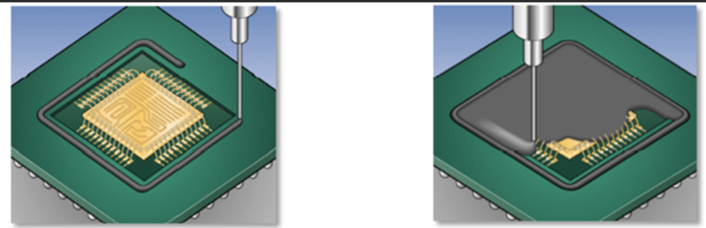
Step 1 – Damming: A highly thixotropic, high-viscosity material is dispensed around the silicon die area. This material functions as a stable “dam,” maintaining its shape immediately after deposition without spreading across the PCB surface. The dam defines and confines the encapsulation region.
Step 2 – Filling: Once the dam structure is completed, a low-viscosity filling compound is dispensed inside the enclosed area. Due to its excellent flowability, the material can self-level and penetrate even the narrowest gaps beneath the die and around delicate wire bonds.
Key Advantages Compared to Other Encapsulation Methods
Although Dam & Fill requires a more complex two-step process, it delivers several critical technical advantages for modern electronic manufacturing.
- Precise Shape Control: The process produces a highly uniform and flat encapsulation surface with consistent height control, making it ideal for thin-profile portable electronics with strict dimensional tolerances.
- Superior Wire Bond Protection: The low-viscosity fill material completely surrounds ultra-fine gold or aluminum wire bonds without causing wire sweep or mechanical deformation — a common risk in transfer molding processes.
- Large-Area Coverage Capability: Dam & Fill can protect larger PCB regions or encapsulate multiple dies within a single protective structure.
- Void Management: Combining low-viscosity fill materials with PCB preheating (typically 60–110°C) allows trapped air bubbles to escape more efficiently, resulting in dense encapsulation with enhanced moisture resistance and thermal shock reliability.
Material Science Behind Dam & Fill Technology
Modern COB encapsulation systems are primarily based on epoxy chemistry due to their excellent mechanical strength and long-term stability.
- Dam Materials: Typically contain high filler loading to reduce the Coefficient of Thermal Expansion (CTE), improving structural rigidity and adhesion strength to the PCB substrate.
- Fill Materials: Utilize ultra-fine fillers to maintain excellent penetration capability while still providing effective thermal conductivity and electrical insulation.
Both materials must maintain strict ionic purity standards to prevent electrochemical corrosion and ensure long-term chip reliability.
Typical Applications
Dam & Fill technology is widely preferred for applications requiring extreme reliability and minimal installation space, including:
- Smart Cards: Applications requiring ultra-flat and ultra-thin chip protection structures integrated directly into card bodies.
- Multi-Chip Modules (MCM) and BGA Packages: Protection for complex electronic assemblies used in telecommunications and automotive electronics.
- Portable Devices: Enhances durability of COB components in smartphones, digital cameras, and medical devices through excellent resistance to shock and vibration.
Selection of Encapsulation Materials
Epoxy Encapsulant Systems
Epoxy encapsulants are the most widely used and industry-standard protection materials for Chip-on-Board (COB) packaging due to their combination of high mechanical strength, excellent adhesion, and long-term environmental stability.
Chemical and Mechanical Characteristics
- Thermoset Nature: Epoxy is a thermosetting polymer that forms irreversible cross-linked molecular structures after curing. This gives the material exceptional rigidity and prevents reflow even at elevated temperatures.
- Mechanical Protection: Epoxy creates a hard protective shell with superior resistance to impact, vibration, and moisture ingress compared to silicone or acrylic systems.
- Excellent Adhesion: Epoxy provides outstanding molecular bonding across various substrate materials, helping prevent delamination — one of the leading causes of chip failure.
Common Hardening Systems
The choice of curing system directly affects thermal performance and manufacturing efficiency.
- Anhydride Systems: The most common curing chemistry for Glob Top applications, offering the highest reliability in harsh environments such as automotive and military electronics.
- Amine Systems: Frequently used for lower-temperature or faster-curing applications.
- Phenolic Systems: Commonly used in molding compounds, typically requiring slower curing and extended post-bake processes. These systems generally exhibit higher CTE and lower glass transition temperature (Tg)compared to anhydride and amine systems.
Processing Classification
- One-Part Epoxy: Ready-to-use materials with virtually unlimited working life at room temperature, requiring thermal curing — commonly around 125°C, with newer formulations curing at lower temperatures such as 80°C.
- Two-Part Epoxy: Requires accurate mixing ratios and has limited pot life after mixing. However, it can fully cure at room temperature or with mild heating for faster processing.
- UV-Curable Epoxy: Enables ultra-fast curing within seconds to minutes, ideal for highly automated production lines.
Role of Fillers in Epoxy Systems
Pure epoxy resin typically has a significantly higher Coefficient of Thermal Expansion (CTE) than silicon dies or gold wire bonds. Therefore, mineral fillers are incorporated to optimize reliability.
- Silica and Alumina Fillers: Reduce CTE mismatch between the encapsulant, silicon chip, and PCB substrate, minimizing thermal stress and crack formation.
- Thermal Management: Alumina fillers additionally improve thermal conductivity, helping dissipate heat from the chip.
Performance in Harsh Environments
Under severe reliability testing conditions such as 85% humidity and thermal cycling from -40°C to +125°C, epoxy systems — especially anhydride-based formulations — demonstrate excellent dimensional stability, minimal moisture absorption, and high shear strength retention. This makes epoxy the preferred choice for applications requiring long-term reliability.
Silicone Encapsulation Systems
Silicone encapsulants provide a highly flexible alternative to epoxy, particularly suitable for COB devices exposed to extreme thermal and mechanical stress. While epoxy prioritizes rigidity, silicone focuses on stress absorption and vibration damping.
Mechanical and Thermal Characteristics
- Outstanding Flexibility: Silicone is significantly softer than epoxy, enabling superior absorption of mechanical shock, vibration, and impact.
- Ultra-Low Glass Transition Temperature (Tg): Typically around -60°C, allowing silicone to remain elastic across standard electronic operating ranges from -40°C to +125°C or higher.
- Low Elastic Modulus: Although silicone exhibits very high CTE values, its softness dramatically reduces actual stress transferred to delicate wire bonds during thermal expansion.
Heat Resistance and Corrosion Protection
- Excellent Thermal Stability: Silicone can continuously operate at temperatures approaching 200°C, exceeding most organic encapsulation systems.
- Corrosion Resistance Mechanism: Although moisture permeability is higher than epoxy, silicone forms stable Si-O-Si molecular bonds on substrate surfaces that help suppress corrosion.
Technical Considerations
- Siloxane Migration: Low-molecular-weight siloxanes may migrate from the material and contaminate nearby surfaces, potentially affecting adhesion or cleaning processes in subsequent manufacturing stages.
- Silicone Contamination Risk: Migration can also interfere with optical components or electrical contacts in sensitive applications.
- Chemical Resistance: Silicone generally exhibits lower solvent resistance compared to epoxy and is typically more expensive.
Processing and Applications
Silicone encapsulants are available in one-part RTV, two-part, and dual-cure UV/moisture systems to support various production requirements.
- Silicone Glob Top: Commonly used for chips with extremely stress-sensitive wire bonds.
- Module Protection: Certain RTV silicones additionally provide EMI/RFI shielding capabilities for electronic housings.
Polyurethane Encapsulation Systems
Polyurethane encapsulants are highly effective when applications require flexibility and stress relief. Compared to epoxy, polyurethane systems are generally softer and better suited for fluctuating environmental conditions.
Key Mechanical Advantages
- High Flexibility: Polyurethane maintains excellent elasticity, particularly at low temperatures, enabling effective shock and vibration absorption without cracking.
- Stress Relief Capability: Its low elastic modulus helps protect sensitive wire bonds from stress caused by thermal expansion mismatch.
- Strong Adhesion: Polyurethane bonds well to various substrates, forming durable environmental protection barriers.
Typical Applications
- Potting: Widely used to encapsulate entire PCB assemblies inside housings for electrical insulation and mechanical protection in industrial and automotive systems.
- Conformal Coating: Polyurethane coatings provide reliable protection against moisture and chemicals, with curing options including heat, moisture, or UV.
Limitations and Reliability Considerations
- Thermal Stability: Continuous operating temperature is generally lower than silicone, typically around 130°Cdepending on formulation.
- Moisture Absorption: Some polyurethane systems exhibit greater weight change and reduced moisture resistance compared to anhydride epoxy systems under 85°C / 85% RH testing.
- Hydrolysis Risk: Certain formulations may chemically degrade after prolonged exposure to high humidity and elevated temperatures.
Curing Systems
- Two-Part Systems: Cure at room temperature or under mild heat, commonly used for large-scale potting applications.
- UV-Curable Systems: Enable curing within seconds for high-speed automated production lines.
Overall, polyurethane is an ideal choice when COB assemblies must withstand strong impact, vibration, or low-temperature operation requiring flexible protection.
UV Acrylic Encapsulation Systems
UV-curable acrylic encapsulants represent a major advancement in COB protection technology by delivering extremely fast processing speed and superior manufacturing control. Unlike traditional thermal curing systems, these materials transition from liquid to solid almost instantly under UV exposure.
Chemical Structure and Mechanism
UV acrylic systems are composed of monomers, oligomers, and photoinitiators.
The material remains liquid until UV light activates the photoinitiators, triggering rapid polymerization and forming a durable solid network. This process provides both structural stability and environmental protection for COB devices.
Core Advantages in COB Packaging
- Ultra-Fast Processing: Curing occurs within seconds instead of hours in thermal ovens, dramatically improving automated manufacturing throughput.
- Cure-on-Demand Capability: Since curing only begins under UV exposure, technicians can precisely position chips and wire bonds before final fixation.
- Protection for Heat-Sensitive Components: Room-temperature curing eliminates thermal damage risks associated with high-temperature ovens.
- Energy and Space Savings: UV curing systems reduce factory energy consumption and eliminate the need for large thermal curing equipment.
Dual-Cure Technology for Shadow Areas
A key limitation of UV systems is that UV light cannot penetrate shadowed regions beneath chips or wire bonds.
Modern dual-cure systems combine UV curing with secondary mechanisms such as thermal or moisture curing. UV rapidly hardens exposed surfaces, while the secondary curing process fully solidifies material in shadowed areas to ensure complete encapsulation reliability.
Typical Applications
- UV Glob Top: Provides thick protective coatings with strong mechanical protection and moisture resistance.
- Precision Sealants: Suitable for applications requiring accurate shape control and excellent adhesion to plastic or gold substrates.
In summary, when high production throughput and protection of heat-sensitive components are the top priorities, UV-curable acrylic encapsulants represent one of the most effective solutions available today.
Key Technical Criteria Determining Encapsulation Performance
| Technical Criteria | Function / Importance | Risk if Not Optimized | Engineering Solution / Requirement |
|---|---|---|---|
| Coefficient of Thermal Expansion (CTE) | Measures how much the encapsulant expands or contracts with temperature changes | Large CTE mismatch between the encapsulant, silicon die, and PCB can generate internal stress, leading to cracks or wire bond failure | Use highly filled encapsulation materials to reduce CTE and better match component expansion characteristics |
| Glass Transition Temperature (Tg) | Defines the temperature at which the material transitions from a rigid to a softer state | If Tg falls within the operating temperature range, mechanical properties may change abruptly and reduce reliability | Tg should remain outside the device operating temperature range to maintain structural stability |
| Adhesion Performance | Determines bonding strength between the encapsulant, chip, and substrate surface | Delamination is one of the most common causes of COB failure | Perform proper surface preparation using solvents, ultrasonic cleaning, or plasma treatment before dispensing |
| Moisture Resistance | Prevents moisture penetration into the chip and wire bond region | Moisture ingress can lead to electrochemical corrosion, leakage current, or short circuits | Select low-moisture-absorption materials and optimize curing conditions to minimize void formation |
| Thermal Conductivity | Supports heat dissipation away from the semiconductor die | Poor thermal transfer may cause heat accumulation and accelerate component degradation | Use thermally conductive fillers such as alumina or specialized ceramic particles |
| Low Ionic Contamination | Ensures chemical purity of the encapsulation system | Ionic impurities may trigger corrosion or electrochemical migration under humidity exposure | Use high-purity electronic-grade encapsulants with tightly controlled ionic content |
| Viscosity and Flowability | Affects the material’s ability to penetrate narrow gaps around wire bonds and beneath chips | Poor flow behavior may trap air bubbles or create incomplete coverage | Match viscosity characteristics to the selected process, such as Glob Top or Dam & Fill |
| Void Control | Ensures dense and uniform encapsulation coverage | Trapped voids may expand during thermal cycling and damage the package structure | Apply PCB preheating and controlled dispensing parameters to release trapped air efficiently |
| Mechanical Modulus | Determines material rigidity or flexibility under stress | Excessively rigid materials may crack under vibration, while overly soft materials may provide insufficient protection | Select encapsulants with mechanical properties appropriate for the target application environment |
| Curing Stability | Ensures complete and consistent polymerization of the encapsulant | Incomplete curing may reduce adhesion, chemical resistance, and long-term reliability | Optimize curing temperature, UV exposure, or dual-cure mechanisms according to material specifications |
Adhesive Dispensing Process and Quality Control
Dispensing technology plays a critical role in ensuring encapsulation reliability for COB protection systems. Modern dispensing platforms are designed to provide highly accurate material control, minimize process variation, and reduce defect risks during production.
Modern Dispensing Technologies
- Syringe Valve Systems:
A simple pneumatic-pressure-based dispensing method suitable for applications that do not require ultra-high precision. - Auger Pump Systems:
Utilize shear force to temporarily reduce material viscosity during dispensing, enabling more stable flow control for high-viscosity encapsulants. - True Positive Displacement Pumps:
The most precise dispensing technology available, delivering exact volumetric control regardless of material viscosity or temperature fluctuation.
Void Management
Air voids trapped inside the encapsulation layer can absorb moisture and potentially cause “popcorning” failures during solder reflow processes.
Engineering Solutions
- Perform dispensing under vacuum environments to minimize trapped air.
- Use pressure chambers immediately after dispensing to force air bubbles outward and improve surface flatness.
- Apply PCB preheating to enhance material flow and reduce void formation around wire bonds and chip edges.
Effective void management is essential for ensuring moisture resistance, thermal stability, and long-term package reliability.
Emerging Trends: UV-Curable Materials and Smart Manufacturing
The transition toward high-efficiency and sustainable electronics manufacturing is accelerating the adoption of UV-curable encapsulation systems.
Advantages of UV Technology
- Ultra-Fast Processing Speed:
UV materials cure within seconds rather than hours required for conventional thermal curing, significantly reducing production bottlenecks. - Energy Efficiency:
Eliminates the need for continuously operating thermal ovens, helping reduce both carbon emissions and operational costs. - Improved Manufacturing Flexibility:
UV systems support highly automated production environments with better process consistency and throughput.
Dual-Cure Technology
One major limitation of standard UV curing is the inability of UV light to penetrate shadowed regions beneath chips or wire bonds.
To solve this challenge, modern encapsulation materials incorporate Dual-Cure Technology, combining UV curing with secondary curing mechanisms such as thermal or moisture curing.
This approach allows:
- Rapid surface fixation through UV exposure
- Complete curing inside shadowed areas over time
- Enhanced reliability across the entire encapsulation structure
As a result, dual-cure systems ensure that every critical area of the COB package receives complete protection, even in highly complex electronic assemblies.