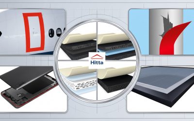
Solution Overview
Electrically conductive tapes combine bonding, electrical connection, grounding, and EMI shielding in a thin, flexible, and customizable construction.
Tape selection should be based on electrical requirements, substrate compatibility, available space, mechanical performance, environmental conditions, and converting capabilities.
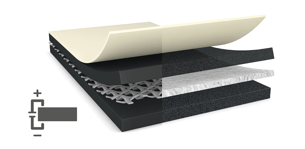
Electrically Conductive Tape (ECT) combines mechanical bonding and electrical conductivity in a single material. Its construction typically consists of a conductive pressure-sensitive adhesive (PSA) combined with one of the following backings:
| Backing | Key Characteristics |
|---|---|
| Woven | High strength and mechanical stability |
| Non-woven | Soft, flexible, and suitable for die-cutting |
| Copper/Aluminum | High electrical conductivity and EMI shielding |
| Conductive Foam | Gap compensation and vibration damping |
| Solution | Function | Applications |
|---|---|---|
| Double-sided | Bonding + grounding | FPC, PCB/MLB, antennas, cameras |
| Single-sided | EMI shielding + grounding | IC/CPU, FPC, cables |
| Conductive Foam | Gap filling + grounding | PCBs, metal frames |
Technical Evaluation
The following parameters should be evaluated together:
Z-axis conduction: Electrical conductivity through the thickness of the tape.
Planar conduction: Electrical conductivity along the surface of the tape.
Shielding Effectiveness (dB): The tape’s ability to attenuate electromagnetic interference (EMI).
Adhesion & mechanical stability: Bond strength and mechanical stability under application conditions.
Environmental resistance: Resistance to heat, humidity, chemicals, and thermal cycling.
Values for electrical resistance, shielding effectiveness, thickness, and adhesion should be verified for each specific product grade and under the applicable test conditions.
FPC grounding
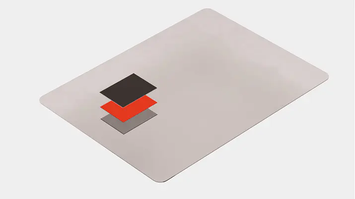
components grounding
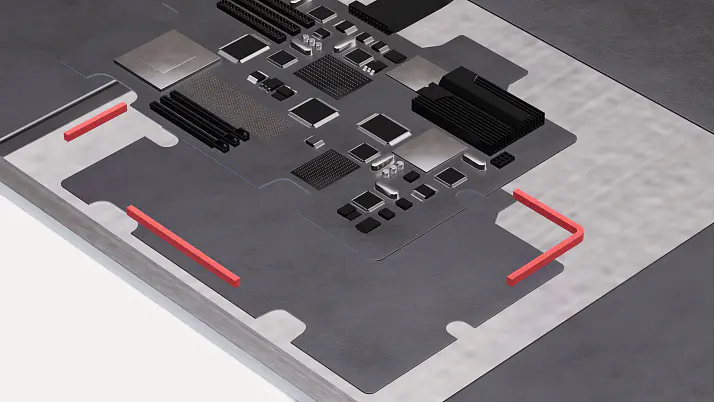
MLB grounding
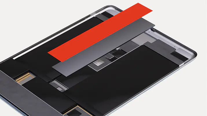
MLB shielding
Applications
- Grounding: FPCs, PCBs, antennas, cameras
- EMI Shielding: IC/CPU components, modules, cables
- Gap Filling & Shock Absorption: Compensating for gaps while maintaining electrical contact
- Wire Wrapping & Conductive Gasketing: Shielding, grounding, and gap management
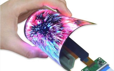
Electrically conductive tapes are widely used in consumer electronics, OLED displays, telecommunications, automotive and eMobility, industrial equipment, and medical devices.
Contact Information
HITTA is a conductive tape solution provider offering products from leading brands such as tesa and BowTape, supporting applications including electrical connection, grounding, EMI/EMC shielding, and electronic assembly.
Beyond material supply, HITTA works closely with manufacturers to analyze technical requirements, select the right conductive tape for specific substrates and operating conditions, and customize solutions for individual production stages. With our Tape Converting capabilities, we can provide customized formats such as die-cut parts, custom-sized tapes, finger-lift tabs, spooled rolls, and other configurations for manual, semi-automated, or automated assembly processes.
Our technical team works directly with customers to identify solutions that meet requirements for electrical conductivity, adhesion, grounding, EMI shielding, and assembly reliability. From initial trials and sample evaluation to mass production, we focus on improving assembly efficiency, ensuring product consistency, and optimizing production costs.
If your business is looking for conductive tape solutions for electronic devices, electronic components, or applications requiring electrical connection and EMI shielding, HITTA can work with you to develop a solution tailored to your technical requirements and actual production process.
Contact HITTA today to discuss your application and evaluate the right conductive tape solution.
☎️ Hotline: 0565.336.879
✉️ Email: hitta@hitta.vn
Controlling Electromagnetic Interference (EMI) and Electrostatic Discharge (ESD) in Modern Electronic Devices
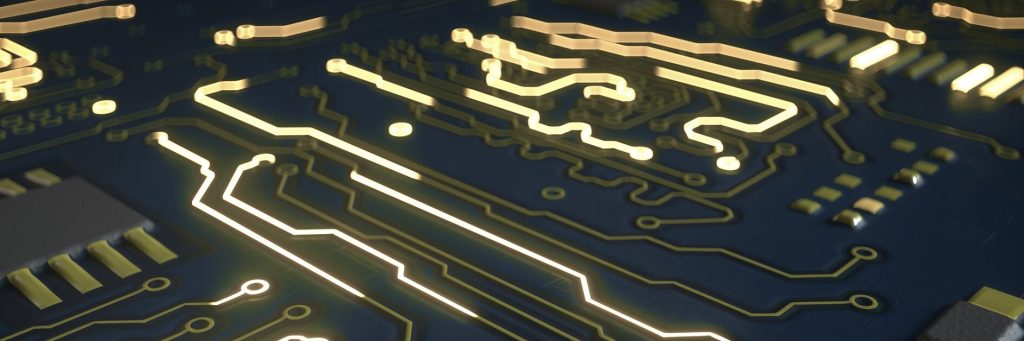
Electronic devices are becoming increasingly compact while integrating more components, higher processing speeds, and higher operating frequencies. Smartphones, tablets, OLED displays, wearable devices, and automotive electronic systems must process large amounts of data and signals within increasingly limited space.
As processors, power circuits, and power components operate at higher frequencies, rapid current switching can generate electromagnetic interference (EMI) and radio-frequency interference (RFI). If not properly controlled, this interference can affect signal transmission, reduce image and audio quality, cause interference between circuits, and even compromise the overall stability of the device.
In addition to EMI/RFI, electrostatic discharge (ESD) is another critical consideration in the design and assembly of electronic devices. Static charges from the surrounding environment or users can be transferred to sensitive components, potentially causing damage or reducing the reliability of integrated circuits (ICs).
As available assembly space continues to decrease, the use of appropriate shielding and conductive solutions becomes increasingly important. Electrically conductive tape is one solution used to create electrical paths, support grounding, provide EMI/RFI shielding, and control static charges directly during the assembly process.
From Traditional Mechanical Connections to Electrically Conductive Tape
Traditionally, grounding and EMI shielding in electronic devices were often achieved using mechanical methods such as rivets, screws, metal clips, or soldering. While these solutions remain suitable for many applications, they can present certain limitations as devices become thinner, lighter, and more highly integrated.
Space and weight requirements: Screws, clips, and other metal components require dedicated installation space, while modern device designs increasingly prioritize thin, lightweight structures and efficient use of internal space.
More complex assembly processes: Operations such as screw fastening, clip installation, and soldering require additional process steps and supporting equipment. In high-speed production lines, this can increase assembly time and make automation more challenging.
Limited suitability for thin and flexible components: The clamping force or fixed points created by screws and clips can introduce stress to surrounding components, particularly displays, FPCs, and other thin or flexible structures.
Against this backdrop, Electrically Conductive Tape (ECT) has become a suitable solution for many electronic assembly applications. It combines two functions in a single material: providing adhesive bonding while also creating an electrical path between contact surfaces.
With its thin, flexible construction and ability to be converted into the required size or shape, electrically conductive tape can be applied in space-constrained areas while supporting requirements for grounding, EMI/RFI shielding, and electrostatic control. This makes it increasingly relevant for compact electronic devices and assembly processes where space optimization is a key consideration.
What Is Electrically Conductive Tape?
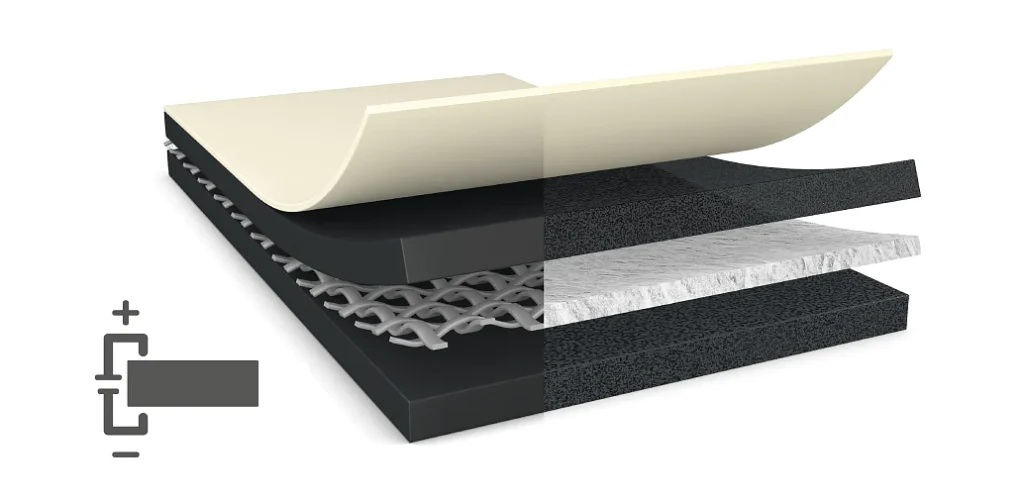
Electrically conductive tape is a type of engineered adhesive material designed to provide bonding between surfaces while maintaining electrical conductivity. The tape typically consists of a pressure-sensitive adhesive (PSA)containing conductive components, combined with a suitable backing such as woven fabric, non-woven fabric, metal foil, or conductive foam.
Depending on its construction and application requirements, electrically conductive tape can perform several functions in electronic devices:
- Electrical Connection and Grounding: Creates an electrical path between components, shielding layers, and metal frames, helping dissipate electrical charges and route unwanted currents to a grounding point.
- EMI Shielding: Helps prevent electromagnetic interference from entering sensitive areas while limiting interference generated within the device from affecting surrounding circuits.
- Component Bonding and Fixation: In addition to providing electrical conductivity, the adhesive layer secures components during assembly. Its thin and flexible construction allows it to bond to a wide range of surfaces, including areas with limited installation space.
Rather than requiring separate solutions for bonding and electrical connection, electrically conductive tape can perform both functions simultaneously, helping simplify product design and assembly processes across a wide range of electronic applications.
Technical Mechanisms of Electrically Conductive Tape
Selecting the right electrically conductive tape for a specific application requires more than simply considering electrical conductivity. It is also important to understand how current flows through the tape, its shielding performance, adhesion, and stability under actual operating conditions.
| Property | In simple terms | Important when |
|---|---|---|
| Z-Axis Conductivity | Electricity can flow through the thickness of the tapefrom one side to the other | An electrical connection is required between two surfaces |
| Planar Conductivity (XYZ-Axis) | Electricity can travel across the surface of the tape | A conductive path is required over a larger area |
| Contact Resistance | The level of electrical resistance encountered as current passes through the tape | Lower values are generally preferred for electrical connections |
| Surface Resistance | The level of electrical resistance encountered as current flows across the material surface | Lower values generally facilitate current distribution |
| Shielding Effectiveness (dB) | The ability to attenuate electromagnetic interference | Higher dB values generally indicate greater shielding effectiveness |
Z-Axis and Planar Conductivity
Electrically conductive tapes can be designed to conduct electricity in one or multiple directions, depending on the construction of the adhesive and backing.
Z-Axis Conductivity refers to the ability to conduct electricity perpendicular to the tape surface, allowing current to flow from one side to the other through the full thickness of the tape. This characteristic is particularly important when the tape is used for grounding or establishing an electrical connection between two surfaces, such as connecting an FPC to a metal frame or between shielding layers within a device.
XYZ-Axis / Isotropic Conductivity allows current to flow both laterally and through the thickness of the tape. This capability is suitable for applications requiring a continuous conductive path across a larger area, such as EMI shielding or conductive contact layers.
Therefore, when selecting an electrically conductive tape, it is important to determine whether the application requires Z-axis conductivity or conductivity across the entire plane of the material.
Contact Resistance and Surface Resistance
Two commonly evaluated parameters for electrically conductive tapes are Contact Resistance and Surface Resistance.
Contact Resistance indicates the resistance to current flow through the tape in the Z-axis direction. Lower values generally indicate better electrical connectivity between two surfaces. This parameter is particularly important for grounding, component interconnection, and electrical contact between different material layers.
Surface Resistance indicates the resistance to current flow across the surface of the material. Lower surface resistance allows current to distribute more easily across the surface, supporting applications that require EMI shielding and dissipation of unwanted electrical currents.
It is important to note that resistance values should not be evaluated in isolation. The measurement method, tape construction, contact materials, and test conditions can all affect the results.
Electromagnetic Shielding Effectiveness
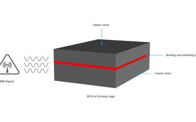
Shielding Effectiveness (SE) is an important parameter when electrically conductive tape is used for EMI shielding. Expressed in dB (decibels), it indicates the degree to which electromagnetic energy is attenuated as it passes through a shielding material.
In principle, higher dB values indicate greater attenuation of electromagnetic interference. However, actual shielding performance depends not only on the tape itself but also on the overall system design, operating frequency, contact configuration, and the ability to maintain electrical continuity at joints and interfaces.
Therefore, when selecting tape for EMI applications, it is important not to consider a single dB value alone. The frequency range, test method, and actual application conditions should also be taken into account.
Adhesion, Mechanical Strength, and Environmental Resistance
In addition to electrical performance, electrically conductive tape must provide reliable adhesion and remain stable throughout its service life.
Peel Adhesion: Indicates the tape’s ability to maintain a bond with the substrate. Performance depends on the adhesive chemistry, substrate material, contact time, and environmental conditions. In electronic applications, stable adhesion helps maintain electrical contact and minimize edge lifting or loss of electrical continuity during use.
Mechanical Strength and Dimensional Stability: Backings such as woven fabric, non-woven fabric, or metal foil can help the tape maintain its shape and withstand mechanical forces during processing. These properties are particularly important when the tape is die-cut, slit-to-size, or converted into complex shapes.
Temperature and Environmental Resistance: Depending on its construction, electrically conductive tape can be designed to operate under different temperature, humidity, and environmental conditions. For electronic devices, the ability to maintain adhesion and electrical conductivity after thermal cycling, exposure to humidity, and other environmental stresses is important for long-term stability.
An effective electrically conductive tape solution therefore needs to provide more than good electrical conductivity. It must also meet requirements for electrical contact, EMI shielding, adhesion, mechanical strength, and environmental stability. The appropriate tape should be selected based on the device construction and the specific requirements of each application.
Electrically Conductive Tape Constructions and Adhesive Technologies
| Construction | Common Materials | Key Characteristics | Typical Applications |
|---|---|---|---|
| Fabric Backing | Woven, non-woven fabric | Mechanical strength, dimensional stability, flexibility | Grounding, bonding, EMI shielding |
| Metal Foil Backing | Copper, aluminum | Electrical and thermal conductivity, EMI shielding | EMI/RFI shielding, grounding |
| Conductive Foam | Conductive-coated or conductive-filled foam | Elasticity, gap filling, cushioning | Conductive gasketing, electrical contact |
| Conductive Adhesive Layer | Conductive acrylic PSA + conductive particles/materials | Adhesion and electrical conductivity | Grounding, bonding, ESD control |
Depending on the requirements for electrical conductivity, adhesion, flexibility, and assembly conditions, electrically conductive tapes can use different backing materials and adhesive systems. Each construction is suited to specific applications across electronics, automotive, display, and EMI/ESD control systems.
Conductive Pressure-Sensitive Adhesive (PSA)
The adhesive layer provides both mechanical bonding and an electrical path between the tape and the surface being connected.
A common construction uses a conductive acrylic adhesive, in which the adhesive is combined with conductive particles or materials such as nickel, copper, or silver. These conductive components are dispersed throughout the adhesive system to establish a stable electrical path while maintaining sufficient adhesion.
A key challenge in conductive adhesive technology is balancing electrical conductivity and adhesion. If the concentration of conductive material is too low, electrical performance may not meet the application requirements. Conversely, excessive conductive filler can affect the adhesive’s flexibility, adhesion, and processability.
Conductive Woven Backing
Conductive woven backings typically use synthetic fibers that are treated or coated with conductive materials.
This construction provides good mechanical strength and tear resistance, while maintaining dimensional stability during converting and use. The woven backing also offers good flexibility, making it suitable for applications where the tape may experience mechanical stress or conform to changing shapes during assembly.
These properties make conductive woven tapes suitable for grounding, EMI shielding, and electrical bonding in applications requiring higher mechanical durability or reworkability.
Conductive Non-woven Backing
Conductive non-woven tape is made from fibers arranged in a non-directional structure and treated with conductive materials.
Compared with woven backings, this construction is generally softer and more flexible, while allowing the adhesive to conform more effectively to the substrate. This can be advantageous when bonding to slightly uneven or non-flat surfaces.
Non-woven backings also offer good converting performance, particularly for die-cutting and forming small, detailed parts. As a result, they are commonly selected for compact electronic components requiring precise tape geometries and installation in space-constrained areas.
Conductive Copper and Aluminum Foil Tapes
Some electrically conductive tapes use copper foil, black-coated copper foil, or aluminum foil as the backing.
A key advantage of these constructions is their high planar electrical conductivity, along with their ability to provide electromagnetic interference (EMI) shielding. Actual shielding performance depends on the product construction, frequency range, and test method, so dB values should be referenced according to the specifications of each individual product.
In addition to electrical conductivity, copper and aluminum provide thermal conductivity and heat spreading, which can support thermal management in certain areas of electronic devices.
For electronic devices with high aesthetic requirements, matte black copper foil is also an option. Its black surface helps reduce light reflection and provides a more uniform appearance when used inside display modules, cameras, or slim electronic devices.
Conductive Foam Tapes
Conductive foam tapes use an elastic foam layer, such as polyurethane (PU) or sponge foam, that is treated or constructed to provide electrical conductivity.
The key difference of this construction is that, in addition to electrical conductivity and grounding, the foam layer can compress and recover its shape, helping maintain electrical contact when there are variations in the distance or geometry between surfaces.
Due to its elasticity, conductive foam can perform several functions simultaneously:
- Grounding: Establishes an electrical connection between components and metal frames.
- EMI Shielding: Helps reduce electromagnetic interference at contact points.
- Cushioning: Absorbs some vibration and mechanical impact.
- Gap Filling: Compensates for uneven gaps or dimensional variations between surfaces.
This construction is particularly suitable for applications where electrical connectivity and mechanical gap compensation are required at the same time.
Depending on the connection location, EMI shielding requirements, and the degree of dimensional variation between surfaces, electrically conductive tapes can generally be divided into three main categories: double-sided conductive tape, single-sided conductive tape, and conductive foam tape.
| Solution Category | Typical Construction | Key Technical Characteristics | Primary Applications |
|---|---|---|---|
| Double-sided Conductive Tape | Conductive adhesive on both sides + woven or non-woven backing | Conductivity through the thickness and across the plane; thin construction; combines bonding and electrical connection | FPC and PCB grounding; securing cameras, antennas, and components requiring electrical connection |
| Single-sided Conductive Tape | Conductive adhesive + copper, aluminum, or conductive fabric backing | Good surface conductivity; EMI shielding; may also provide thermal conductivity depending on the backing material | IC/CPU shielding; signal cable wrapping; FPC shielding and grounding |
| Conductive Foam Tape | Conductive adhesive + elastic conductive foam layer | Compression and recovery; compensates for dimensional gaps; combines electrical conductivity with mechanical cushioning | Gap filling between PCBs and metal frames; grounding; conductive gasketing; vibration and impact damping |
Applications of Electrically Conductive Tape
Electrically conductive tape is used in a wide range of locations within electronic devices, from grounding and EMI shielding to gap compensation and mechanical protection. Depending on the location and technical requirements, double-sided, single-sided, or conductive foam constructions can be selected.
| Application | Primary Function | Description |
|---|---|---|
| FPC & PCB/MLB Grounding | Grounding and electrical connection | Connects FPCs, PCBs, or MLBs to metal frames, providing a stable electrical path to ground |
| Antenna & Camera Grounding | Grounding and interference control | Supports electrical connection for antenna and camera assemblies and related components while helping control electromagnetic interference |
| EMI Shielding for ICs/CPUs | Electromagnetic interference shielding | Provides a conductive layer over areas that generate or are susceptible to EMI, helping limit interference propagation within the device |
| Gap Filling & Shock Absorption | Gap compensation and cushioning | Conductive foam compresses and recovers to maintain electrical contact between uneven surfaces while absorbing some vibration and mechanical impact |
| Wire Wrapping & Gasket Sealing | Cable wrapping, electrical contact, and shielding | Used to wrap cables and wires or address areas requiring electrical contact, EMI shielding, and limited gap sealing |
FPC Grounding and PCB/MLB Grounding
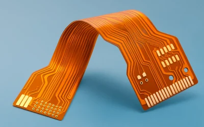
Flexible printed circuits (FPCs) are used to connect various component assemblies, including displays, touch panels, cameras, and other modules, to the main PCB/MLB. Because FPCs are often routed through tight spaces and may need to flex during assembly and operation, maintaining reliable electrical connectivity and EMI control is an important design consideration.
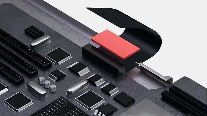
Application: Double-sided conductive tape, typically using a woven or non-woven backing, can be die-cut to the required shape and applied to designated contact areas on the FPC. During assembly, the tape establishes an electrical connection between the FPC and the metal frame or grounding point of the device.
Benefits: Provides a stable electrical path between the FPC and metal frame, supporting grounding, charge dissipation, and EMI control. At the same time, the tape provides mechanical fixation without requiring additional metal components.
Antenna and Camera Module Grounding
Camera modules and antenna systems such as 5G, Wi-Fi, and Bluetooth are typically installed in highly space-constrained areas and may be located close to multiple electronic components. As a result, grounding and electromagnetic interference control are important considerations during device design.
Application: Thin electrically conductive tape can be precisely die-cut to match the shape of the mounting base, contact area, or perimeter of the module. The tape can establish an electrical connection between the metal portion of the module and the device frame or grounding point on the PCB.
Benefits: Helps maintain a stable ground connection, reduce unwanted current paths, and support EMI control around antenna, camera, and adjacent electronic circuits.
EMI Shielding for CPUs and ICs
CPUs, power management ICs, and high-frequency circuits can be sources of electromagnetic interference within electronic devices. These areas are often protected using shielding cans or other metal shielding structures.
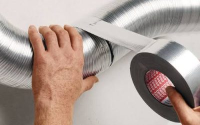
Application: Single-sided conductive tape with copper foil, aluminum foil, or conductive fabric backing can be used to cover areas requiring shielding or to address contact points and gaps between metal components.
Benefits: Adds a conductive layer that supports EMI shielding and grounding, helping limit electromagnetic interference between different areas of the device. Actual shielding performance depends on the overall system design, operating frequency, shielding structure, and the quality of electrical contacts and grounding points.
Conductive Gap Filling & Shock Absorption
In compact 3D device structures, the distance between the PCB/MLB and metal frame may vary due to manufacturing and assembly tolerances. If a material is too rigid or unable to compensate for these gaps, electrical contact may become inconsistent.
Application: Conductive foam tape is placed at locations where an electrical connection is required between the circuit board and metal frame. When the device housing is assembled, the foam compresses to compensate for dimensional variations and provide appropriate contact pressure.
Benefits: Maintains electrical contact despite variations in the gap between surfaces, while the foam layer can also absorb some vibration and mechanical impact. This is particularly valuable in handheld devices and applications requiring high mechanical stability.
Wire Wrapping and Conductive Gasketing
Within electronic devices, cables and signal lines may pass through multiple areas of the enclosure. If these locations are not properly treated, they can become potential paths for electromagnetic interference to radiate or leak.
Application: Conductive fabric tape can be used to wrap cable bundles or wires, while conductive foam materials can be formed to address areas requiring electrical contact and gap compensation.
Benefits: Helps create a conductive shield around cables, connect them to a grounding area, and reduce potential EMI leakage through mechanical gaps. For designs with stringent EMC requirements, the material construction, grounding points, and assembly method should be considered as an integrated system.
Applications Across Multiple Industries
In addition to smartphones and consumer electronics, electrically conductive tape is used across a wide range of industries requiring grounding, EMI shielding, ESD control, and electrical connectivity in space-constrained applications.
| Industry / Sector | Typical Applications |
|---|---|
| Automotive & eMobility | BMS, ECUs, sensors, radar/LiDAR, center displays, electrical systems, and electronic modules requiring EMI control |
| Consumer Electronics | Smartphones, tablets, laptops, smartwatches, TVs/displays, and IoT devices |
| Medical Devices | Monitoring equipment, diagnostic devices, and electronic systems requiring interference control |
| Aerospace & Aviation | Avionics, communication systems, control systems, and modules requiring shielding and grounding solutions |
| Industrial Equipment | Controllers, sensors, automation equipment, and industrial electronic systems |
Across all of these industries, electrically conductive tape should not be selected based on electrical conductivity alone. Adhesion, backing construction, converting capabilities, mechanical stability, temperature resistance, and shielding performance under actual operating conditions should all be considered when determining the appropriate solution.
Criteria for Selecting Electrically Conductive Tape Solutions for Design Engineers
Selecting electrically conductive tape involves more than evaluating electrical conductivity. To ensure stable performance in the final product, design engineers need to consider electrical requirements, available assembly space, bonding surfaces, mechanical loads, and environmental conditions together.
| Step | Evaluation Criteria | Parameters / Questions to Check |
|---|---|---|
| 1. Define electrical requirements | Electrical conductivity and EMI shielding | Is conductivity required through the Z-axis or across the surface? What Contact Resistance is required? What level of Shielding Effectiveness is needed, and at which frequency range? |
| 2. Evaluate space and geometry | Thickness, shape, and gap | How much assembly space is available? Is the bonding surface flat or curved? Is gap compensation or material compression required? |
| 3. Evaluate bonding surface and mechanical load | Adhesion and mechanical stability | Is the surface SUS, aluminum, PC, ABS, PET, or another material? Is it an LSE or rough surface? Will the tape be exposed to tensile or bending forces, or to edge lifting and peel stress? |
| 4. Check environmental conditions | Temperature, humidity, and chemicals | What is the operating temperature? Will the application be exposed to thermal cycling, high humidity, sweat, or chemicals? |
| 5. Validate through actual testing | Stability after assembly | Test adhesion, electrical resistance, EMI shielding, and durability under environmental and mechanical conditions appropriate to the product. |
Addressing Space Constraints and Material Thickness
Available assembly space is one of the first factors to determine. This is particularly important for smartphones, camera modules, displays, and other thin electronic devices, where even a few tenths of a millimeter can affect the overall design.
When the gap between two surfaces is very small and relatively flat, double-sided conductive tape with a thin backing, such as non-woven or woven fabric, can be considered. These thin constructions provide an electrical connection without significantly increasing the thickness of the component assembly.
In contrast, when the gap varies or is uneven, conductive foam tape may be more suitable because it can compress and recover to accommodate dimensional variations. The compression ratio should be determined based on the design, material thickness, and required contact force for each application, rather than applying a fixed compression level across all products.
Evaluating Interference Frequency Ranges and EMI Shielding Effectiveness
Not all sources of interference have the same characteristics. Devices using 5G, Wi-Fi, Bluetooth, or high-frequency switching power circuits may generate interference across different frequency ranges.
Therefore, when selecting tape for EMI shielding, it is important to evaluate Shielding Effectiveness (dB) across the frequency range relevant to the application, rather than relying on a single dB value.
In addition to the backing material, shielding performance also depends on the shielding design, grounding method, contact area, joints, and gaps. In some applications, copper foil or conductive fabric may be preferred because they can provide a continuous conductive layer over a larger area.
Evaluating Bonding Surfaces and Mechanical Loads
Bonding surfaces may include stainless steel (SUS), aluminum, copper, PC, ABS, PET, glass, and other materials. Each surface has different surface energy and adhesive interaction characteristics.
For low-surface-energy (LSE) or slightly rough surfaces, an adhesive system with good wetting properties should be selected to increase the actual contact area and maintain stable adhesion.
For applications involving curved surfaces or tape bending, attention should be given to the flexibility of the backing, resistance to edge lifting, and stability after bending. These factors are particularly important for FPCs, cables, and components with complex geometries.
Evaluating Durability Under Temperature, Humidity, and Chemical Exposure
A product may meet performance requirements immediately after assembly, but its ability to maintain those properties throughout its service life also needs to be evaluated.
Depending on the application, testing may include:
| Test Category | Purpose |
|---|---|
| Thermal Cycling | Evaluates the stability of the bond and electrical connection through repeated temperature changes. |
| High Temperature / High Humidity | Evaluates the ability to maintain adhesion and electrical performance under hot and humid conditions. |
| Drop / Impact Test | Evaluates the ability to maintain bonding and electrical contact after impact or dropping. |
| Chemical Resistance | Evaluates the effects of sweat, cleaning solutions, or chemicals that may come into contact with the product during use. |
| Electrical / EMI Test | Verifies contact resistance, grounding performance, and shielding effectiveness under actual application conditions. |
Conditions such as 85°C/85% RH, the number of thermal cycles, compression level, or drop-test conditions should be defined according to the standards and specific requirements of each product. A single test condition should not be treated as a universal standard for all electrically conductive tape applications.
Validating the Solution Through Actual Testing
Once the appropriate construction and specifications have been identified theoretically, the next critical step is to test the material directly on the actual substrate and product design.
A suitable electrically conductive tape solution needs to meet multiple requirements simultaneously:
Electrical Conductivity → Adhesion → EMI Shielding → Mechanical Durability → Environmental Stability → Converting Capability
For applications requiring die-cutting, slit-to-size converting, or complex shapes, the material’s converting capability should also be evaluated from the early selection stage. This helps reduce the risk of having to change materials after the product has already entered mass production.